A nanotube is a cylinder made up of atomic particles and whose diameter is around one to a few billionths of a meter (or nanometers). They can be made from a variety of materials. Nanotubes are believed to be stronger than steel, but more flexible than plastic, and they also exhibit excellent thermal and electrical conductivity. These nanotubes offer the potential to be a fantastic industrial component that could be used to further strengthen infrastructure that we build. More importantly, though, is how they might appear in chips and electrical wiring in the future. Because of their strength and flexibility, they are incredibly beneficial in society, and could revolutionize fields such as nanotechnology, optics, architecture, electronics and materials science. Nanotubes vary by the number of cylinders; there are nanotubes made up of a single cylindrical layer but there are also reinforced nanotubes comprised of two or more cylindrical layers (one nanotube cylinder completely encloses another). Wall thickness also differs; some nanotubes are thicker than others. Since nanotubes vary by wall thickness and number of cylinders, the radius of nanotubes is also variable. Moreover, the length of nanotubes is also not universal. Finally, nanotubes can be organic or inorganic, depending on the particles used in nanotube construction.
Carbon Nanotubes
A carbon nanotube (which is the most popular type of nanotube at the moment) is a cylinder which has a wall of single graphite atoms. Its diameter is exactly one nanometer. A carbon nanotube has exceptional endurance due to its unique sp2 bonding structure. However, at a certain degree of pressure, the nature of the atomic bonding changes and this allows multiple nanotubes to link together and form a longer carbon nanotube chain. Nanotubes of this type are therefore exceedingly strong yet still flexible. Nanotubes made of graphite atoms also have distinctive electrical properties so they can become conductors or semi-conductors in turn. They can be used in the manufacture of capacitors; by using multiple layers, nanotubes become capable of holding electrical charge. They can also be used in the manufacture of resistors and transistors.Multiple cylinders of a single nanotube have been found to work well together. The inner cylinder can actually rotate or move inside the outer cylinder without much resistance from the latter. This characteristic can be applied to make special microscopic rotors. Nanotubes have an amazing potential in a wide variety of fields such as electronics engineering (especially in the manufacture of microscopic chips), optical technologies, nanotechnology, and materials engineering.
Manufacturing Nanotubes
To begin with, a factory that makes nanotubes requires millions of dollars in industrial equipment. In essence, a nanotube factory takes a piece of graphite–whose chemical makeup is almost entirely carbon–and breaks it apart to the point where they can deal in that very thin one atom thick nanometer type of measurement. Once they have that, they are able to coil it together and bunch it up so that they have a very strong nanotube. It’s almost comparable to a spider’s web. The spider continues to weave it together so that it is incredibly strong. There are several approaches to the commercial manufacture of carbon nanotubes. They include the arc discharge method, the laser-aided vaporization method and the chemical vapor deposition (CVD) method. The arc discharge method has been accidentally discovered in 1991 when carbon nanotubes were found in the residue of an electrical arc discharge.
Laser Ablation
The laser-aided vaporization method (commonly known as the laser ablation method) involves a graphite board that’s enclosed within a high-temperature reactor chamber. A laser is then activated and the graphite board is consequently vaporized. All the while, a non-reactive gas is allowed to escape into the reactor chamber. The vapor inside the chamber is then allowed to cool and condense forming carbon nanotubes as a result. Specifically, the nanotubes form on the cool surfaces of the reactor. The size of the tube can be determined by changing the overall temperature of the reactor. In other words, make it hotter and the diameter will be one size and make it cooler and it will be another size. The problem with this method is that it is more expensive than others.

Chemical Vapor Deposition (CVD) Method
To begin with, a substrate is made composed of metal catalyst particles. Iron, nickel or cobalt are the acceptable types. The size of the metal particles determines the diameter of the nanotubes. That’s why the metal is important. This substrate is heated to about 700 degrees Celsius in a vacuum chamber. Two gasses are slowly leaked into the chamber. The first is a process gas such as hydrogen or nitrogen. The second is a carbon containing gas such as ethanol or ethylene. When catalysis occurs at the metal, nanotubes form. Specifically, the catalyst particle breaks apart the carbon containing gas. The carbon moves to the edge of the particle and that’s where the nanotube forms. This method shows much promise, but is still being heavily researched.
How Were Nanotubes Discovered
They are speculated to have been unwittingly discovered in the Middle Ages (1100 to 1700 AD) by the forgers of the famous “Damascus Steel”. Modern research has confirmed the presence of carbon nanotubes and nanowires in the material, and attributes their presence to the forging process that this steel went through.
The modern, scientific discovery of Nanotubes, though, is controversial ground. Sumio Ijima, a scientist from NEC Japan, is widely accepted as the unique discoverer of carbon nanotubes. His paper on the subject, published in the year 1991, threw the spotlight on nanotubes and paved the way for future research on nanotubes in the field of nanotechnology. In recognition of his efforts, he was awarded the Benjamin Franklin Medal in Physics in 2002, and was the co-recipient of the the Kavli Prize for Nanoscience along with Louis Brus (discoverer of colloidal semi-conductor nanocrystals known as quantum dots), in 2008. But, though Mr. Ijima made significant contributions to this field, he is not the first person to have reported about the existence of nanotubes.
As early as 1952, L.V. Radushkevich and V.M. Lukyanovich published photographs of 50 nanotubes along with their research in an issue of the Soviet Union’s Journal of Physical Chemistry. The Soviet Union did not give other countries free access to its scientific research papers, and the article was completely in Russian, limiting the scope of its impact and reach.
M Endo from Japan, who was interested in carbon fibers, collaborated with A Oberlin from France and reported on the observation of carbon nanotubes by electron microscopy in 1976. In 1979, John Abrahamson gave a presentation at Pennsylvania State University eliciting evidence on the existence of nanotubes, planting the seeds for further research in the field. Soviet scientists went for it again in 1981, publishing their findings that nanotubes could be of a cylindrical or spherical structure, which has been proved right today. In 1987, Howard G. Tennett was granted a patent by the government of the United States for the production of a nanotube-like structure.
Therefore, although it is Ijima’s research that ignited interest in nanotubes and led to the rapid research and development that followed, their discovery must be attributed to over 4 decades of research by many known and unknown scientific experts.
How Are Nanotubes Used
Creating Better Pressure Sensitive Conductors with Carbon Nanotubes
Use as pressure sensors is one of the applications of nanotubes. In an experiment where a block of nanotubes was created, the application of an electrical current was provided to test resistance. Resistance to the electrical conduction reduced as more pressure was applied to the nanotube structure. The nanotube structure showed promise up to sixty-five percent compression/stretch length of the original length. The scientists who discovered this use are currently trying to create a polymer which incorporates the nanotubes to make the same pressure sensor ability while increasing the amount that the sensor could be stressed without damaging the connection.
Examination of Composite Materials with Carbon Nanotubes
Since carbon nanotubes are fairly good semi-conductors, they can have electricity passed through them with relative ease. Manufacturers of composite materials often cannot control the cracking and imperfections in their materials. These nano-sized cracks could cause potential problems in the future by lowering the structural integrity of the materials. By spreading the carbon nanotubes onto the surfaces of the composite materials, their structural integrity can be examined and the life of the materials can be determined with various factors. The process is simple and fast and possibly beneficial by adding strength to the composite materials through the electrically induced binding of the nanotubes to the structure.
Artificial Synapse Connections with Carbon Nanotubes
Several scientists in Texas propose that carbon nanotubes could be used towards treating conditions in which neurons are unable to communicate with the body. This technology would also be capable of implementation of prosthetic limbs which could be artificially connected to the body through carbon nanotube technologies. This would allow for cell growth to be stimulated and simulated natural controls of the prosthesis could be achieved. The process would take a large amount of work to make possible and the technologies could take over a few decades to test and perfect. The theoretical process of integrating inorganic materials into the body or placing the brain into an artificial body and life support system may one day be a reality.
Longer Lasting Batteries with Carbon Nanotubes
Carbon nanotubes are very small, but they offer a wide range of area within this small space. The area of the capacitor electrode could be increased with carbon nanotubes without increasing the physical size of the battery. This increased the amount of energy which could be stored on the battery and has an even distribution of the energy, meaning longer life span. This technology makes it possible for fewer wastes to be created and longer lasting batteries. Within a time span of 5 years, it is speculated that ultracapacitors of this type will be available. Revolutionary battery power lengths are expected with carbon nanotubes.
Transparent Conductor Technologies with Carbon Nanotubes
Carbon nanotubes can be created into sheets that are so small and thin, that light passes easily through them. The process of creating these thin sheets of carbon nanotubes is readily available and is very cheap to produce. These ultra-thin sheets of carbon nanotubes have the ability to become transparent conductors which are used by several different imaging technologies. The common devices which use the transparent conductors are:
Televisions – The old cathode ray tube televisions which used RGB colored pixel element illumination with phosphor used different types of transparent conductors which were controlled by the signal and displayed in the appropriate order on the television.
LCD Screens – Liquid Crystal Displays are themselves a type of transparent conductor which uses electrical signals to display the needed colors and levels of light to each and every pixel on the screen.
Plasma Screens – The use of transparent conductors helps to transfer photonic crystal illumination on plasma screens. Plasma screens use free flowing ions to convert into photons which are used to illuminate the colored phosphor.
Touch Screens – Use of touch screen technologies take part in the incorporation of transparent carbon nanotubes. They are placed on the surface of the display to map input by the touch sensors.
Photovoltaic Cells – Solar panels use transparent conductors to be able to absorb more light and transform it into usable electricity. This reduces the reflection of the solar paneling while allowing for maximum absorption of light.
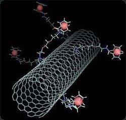
Carbon Nanotubes as a Biomolecule Marker for Cancer Detection
Biocompatible materials such as carbon nanotubes are able to be used for various functions within the body as a medical tool. One of these options is to coat areas that are most likely to be cancerous within the body with the carbon nanotubes as a biomolecule detector. This could then be used to activate the carbon nanotubes and visualized similar to florescent tags but with a much higher accuracy and range of detection. Although this is a great alternative which is very effective, we are yet to know the possible dangers to using carbon nanotubes. Carbon nanotubes may very well be toxic to humans and simply take much longer to create problems within our bodies. It is important for proper testing of this option to take place before it is approved for use as a better detection marker for the masses.
Although the link between cancers is uncertain in humans due to carbon nanotubes, experiments on lab mice have concluded that carbon nanotubes cause cancer like growths. The carbon nanotubes are similar to the needle-like structure of asbestos which affects the lungs in humans as a cancer causing agent. All mice which were exposed to the carbon nanotubes in a controlled setting exhibited cancerous lesions. The amount, if any of carbon nanotubes required to cause similar effects in humans is unknown.
Nerve Cell Signal Carrying and Stimulation
It has been proposed by Scientists in Texas that the ability for nanotubes to be used in the production of cell growth which could be used as a basis for neuron attachment and growth. This could then be used as a possible way to allow for the interaction between organic cellular connections and inorganic prosthesis connections to communicate and interact. Of course this is all theoretical and the application of this technology is not even possible with the current equipment and tools in modern times. The first steps may be experimenting on people who have experienced paralysis or loss of sensation and determining whether or not signals can be processed over the nanotube structures.
Nanotube Use as a Transparent Conductor
Transparent conductors are important in many devices such as televisions and optical touch screens. Their use in solar cells is also regarded as important to produce efficient energy collection. Use of nanotubes as a transparent conductor is possible because of the extremely small amount of material needed to perform well. This means a reduction in the cost of the amount of material as well as a low cost for the material in production making the technology more cost effective.
Use of Nanotubes as Ultracapacitors
When the surface area of a capacitor’s electrodes increases, the amount of energy it can hold increases. This is being tested with nanotubes to significantly increase the amount of surface area in batteries to create long lasting energy and create fewer wastes. The technology to produce these ultracapacitor super batteries should be seen in an estimated 5 years. This could really change the way that our battery operated devices function in the near future.
Possible Toxicity of Nanotubes
The toxicity of nanotubes is not yet fully known or understood. There have been tests done on lab animals which have produced interesting results. It is known that the nanotubes are needle like in structure and acts similarly to asbestos in the lungs of lab mice. The nanotubes create the same conditions which occur in mesothelioma. The inhalation of nanotubes can cause this because of the small size and ability to ingrain themselves into the lungs of the mice. The potential to be as toxic and lethal as asbestos may make products and substances created with nanotubes much more important to control.


Follow Us!