Flash memory is a nonvolatile memory type that is constantly-powered. It has the capability to be reprogrammed or erased in various units of memory referred to as blocks. The technology is based on EEPROM (erasable programmable read-only memory) that is written and erased at the byte level which operates at a much slower rate than flash memory. It is commonly used to store control code such as a computer’s BIOS and supports writing in block sizes making the code easier to update. Compared to RAM (random access memory), the memory type is not considered as easy to use by developers or end-users.
How Does Flash Memory Get Its Name?
Flash memory chips or cards get their name from the method that memory cells can be erased in a single function also referred to as a “flash.” The specific erasing technique is accomplished through Fowler-Nordheim tunneling that uses electrons to remove the electronic charge from a floating gate associated with the targeted memory cell. The electrons pierce a dielectric material to accomplish the removal of the charge.
Flash Memory History
Dr. Fujio Masuoka invented flash memory when her worked for the Toshiba company in 1980. At the time, he invented the two types of memory that are based on NAND and NOR operations respectively. The memory obtained its name from Masuoka’s co-worker or colleague, Shōji Ariizumi, based on the erasing method of the memory reminding him of the flash of a traditional camera. The invention would later be presented at the 1984 IEEE sponsored IEDM in San Francisco, California.
Four year later, Intel introduced the first commercial-based flash chip in 1988 based on the NOR type design. Although the NOR-based chips have longer writing and erasing timeframes, they provide a full data and address bus that allows random access to all memory locations located on the chip. This functionality made the chips a suitable replacement for the legacy ROM chips that were used to store less-updated programming code on a computer such as firmware or computer BIOS’s. The endurance of NOR flash chips eventually grew to range from as few as 100 for on-chip flash memory to 10 to 100k erase cycles and eventually 1,000,000. The NOR-based media was first used and was the basis for CompactFlash.
Eventually, industry has transitioned to NAND-based flash chips due to the decreased write and erase times, less chip area required per memory cell, and lower cost. Additionally, NAND flash memory has a much greater endurance than NOR-based chips. The primary drawback of NAND memory remains the inability to random access of memory on the chip. The information must be accessed on a block-basis that can vary significantly in size. As a result, NAND flash has not become a replacement for NOR-based chips for programmable ROM since the majority of computer microprocessors continue to require byte-level access to memory. NAND flash memory is very similar to other storage devices similar to optical media, MultiMediaCards, and SD cards.
How Does Flash Memory Work?
Flash memory chips or card save data in array(s) of memory cells that are created from floating gate transistors. In a traditional device (single level cell, or SLC), each of the memory cells will only store a single bit of data. Newer flash memory designs are able to store more than one bit of data per cell through the technique of selecting multiple levels of electrical charge to apply to the cell floating gates. Floating gates in flash memory are able to be conductive or non-conductive,
What is a Floating Gate Transistor?
In a flash memory card, every memory cell on the card is similar to a metal–oxide–semiconductor field-effect transistor or MOSFET. The primary difference is that the cell transistor consists of two gates instead of one. On the top of the device is the control gate similar to other MOS transistors. On the bottom is a floating gate that is insulated by an oxide layer around the entire gate. The FG is set in between the control gate and the MOSFET channel of the cell. Since the floating gate is isolated (electrically), all electrons placed on the gate are isolated and can last for a number of years before they will dissolve. Since the floating gate is holding a charge, it will also partially cancel the electric field resulting from the control gate that will further modify the threshold voltage of the memory cell. In order to get a reading from the cell, there is a voltage intermediate between the threshold voltages that is applied to the control gate. The MOSFET channel conductivity is then tested and is further influenced by the floating gate. As the current through the MOSFET channels is sensed, there is a binary code formed that reproduces the stored information in the memory cell.
How Do NOR Flash Memory Internal Charge Pumps Work?
Although there is a significant need for erasing voltages on flash memory chips today, almost all chips only require a single supply voltage and then produce higher voltages using charge pumps that are located on the chip itself. More than half the energy used by a standard 1.8 volt flash chip is lost in the charge pump operation. After a significant amount of research, engineers have found that a boost converter is more efficient than a charge pump and have worked to using a single shared external boost converter on newer chips.
Another issue with on-chip charge pumps is that they are the first part of the chip to fail in a high radiation environment to include spacecraft. The memory on these chips will continue to work in a read only mode at high radiation levels.
NOR-Based Flash Memory
NOR-based flash memory gates ensure each memory cell has a single end directly connected to the ground and the other connected to one of the bit lines. The name of this setup is referred to as “NOR flash” since the arrangement acts similar to a NOR gate. For example, when one of the word lines that is connected to the control gate is at a high condition, the correlating storage transistor will then pull or set the output bit line to low. NOR flash memory is the desired technology for embedded applications that demand the use of non-volatile memory. Due to the low read latencies of NOR flash devices, both data storage and direct code execution can be supported on the same chip.
How to Program a NOR Flash Memory Cell
When a single level NOR flash cell is in its default state, it is logically set to a binary one value. This is due to the fact of current being able to flow through the channel with applying appropriate voltage to the memory cell’s control gate to pull down the bitline voltage. Conversely, a NOR flash memory cell can be programmed to a binary zero value using the following procedure:
Step 1 – Apply an elevated “on” voltage to the control gate (this is normally above five volts in value).
Step 2 – Once the channel is “on,” electrons will now flow from the source of the voltage to the drain if an NMOS transistor is installed.
Step 3 –One the source drain current is high enough, some of the high energy electrons will jump through the insulating layer onto the field gate through a hot-electron injection process setting the value of the NOR flash memory cell to be set to a binary zero.
How to Erase a NOR Flash Memory Cell
In order to conduct an erase operation on a NOR flash memory cell (or reset it to the “one” memory state), there must be a significant or large voltage of the opposite polarity applied in between the source terminal and the control gate. This action will pull the electrons off of the field gate through a quantum tunneling operation. Since newer NOR flash memory chips now have erase segments or blocks of sectors, the erective erase operation is only performed on a block basis requiring all of the cells in the segment to be erased at the same time. Conversely, these same cells can be programmed a single byte or word of memory at a time.
NAND Flash Memory
NAND-based flash memory cards also use floating gate transistors like NOR types; however, they are connected in a method similar to a traditional NAND gate. On this style of flash memory card, there are a number of transistors connected in series. In this arrangement, the bit line is only pulled low if all of the word lines are pulled high. These groupings are then connected via additional transistors in a bit line array similar to a NOR-styled flash chip. This adds an extra level of addressing when compared to the NOR-type resulting in NAND flash memory being able to address memory by both bit, word, or page. This feature allows NAND flash memory to better fit serial programs or applications such as a hard disk that require single bit addressing. When an application is run in-place; however, all of the bits in a word must be accessed at the same time. This operation requires addressing at the word-level.
Although NAND flash memory requires more transistors than NOR flash, the space saved by reducing the total number of bit lines and ground wires allows chip designers to create a more dense chip layout. This results in there being a much larger storage capacity available on each chip as compared to a NOR flash chip. Since manufacturers push the envelope in usable transistor size to maximize storage space on the chip, there is a certain number of faults allowed on NAND flash memory chips. NOR chips; on the other hand, are expected to be error or fault free since they are used for BIOS RAM on some computer motherboards.
How to Erase and Write to NAND Flash Memory
NAND flash memory cards make use of tunnel injection to both write to memory and to use tunnel release for erasing data. This style of flash memory is the technology behind the majority of solid state device drivers, USB drives, and memory card formats make use of the NAND-styled chips today.
What are the Limitations of Flash Memory?
Some of the predominant limitations of flash memory are block erasure, memory wear, and the read disturb problem.
How Does Block Erasure Work?
A significant issue or limitation with flash memory cards are although they are able to be programmed and read at the byte and word level in a random fashion or method, they are only able to erase data at the block level. This operation sets all bits in the corresponding block to a digital one value. When a bit has been programmed to a zero value on older chips, it can only be reset to the one state by erasing the entire block of data that it resides. As a result, although NOR flash provides random access for programming and reading operations, it does not provide the same for rewrite or erase operations. It does allow a bit position to be rewritten as long as new value “zeros” are a super set of the new rewritten information.
The Memory Wear Limitation
Another significant limitation of flash memory cards is the problem of memory wear. Normally, there are a finite or limited number of erase cycles that a flash memory card can undergo. Most commercial products on the market today are rated to withstand approximately 100,000 cycles prior to the chip starting to show the wear and tear of age. In the later portions of the 2000s, there were chips announced that supported reading/writing cycles of more than 1,000,000. The limitation does not typically apply to read-only applications such as routers or thin clients that are not reprogrammed more than a few times during the life of the device.
Read Disturb Limitation
The primary method to read memory on NAND-styled flash memory has been known to cause cells in nearby memory blocks to become programmed or to change over time. This phenomena is known as “read disturb.” In order to avoid this issue, the flash chip controller will normally keep track or count the total number of reads to a memory block since the last time it was erased. Once the designed limit is reached, this block is copied to a new block and then erased and released to the memory block pool. Once this occurs, the original data block is considered ready to use again. If this work-around is not employed in time; however, the read disturb error will happen and there can be data loss as a result.
Types of Flash Cards
Compact Flash Cards
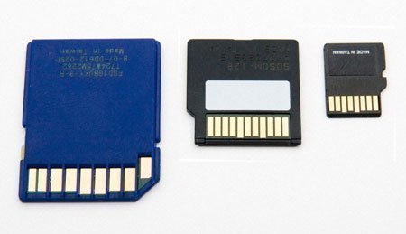
Compact Flash cards, more popularly known as plain CF cards, are typically 36mm x 43mm and weigh around 3.3g. They come in two types, a thin one (around 3.3mm) and a thick one (around 5mm). These two types of CF cards are non-interchangeable because they require different types of card readers. Their storage capacity range from 32 Mb to 32 Gb.
Smart Media Cards
Smart Media cards are typically 45mm x 37mm and weigh around 2 g. They are very thin at only 0.76 mm. They used to be popular in digital photography but they have now been superseded by other media cards. When they were first manufactured, they were styled as the successor to floppy disks. They are compatible with most devices and there are adaptors that enable their use with devices with which they’re not directly compatible. However, Smart Media cards have limited storage capacities with the maximum currently at only 128 Mb.
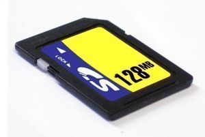
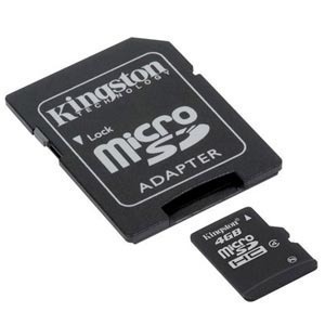
Secure Digital (SD) and Multimedia Cards (MMC)
Secure Digital cards and Multimedia cards look the same as both are around 32mm x 24mm. SD cards, however, are typically thicker and heavier at 2.1mm and 2g, respectively. However, there are now smaller and lighter SD cards popularly known as miniSD cards. SD cards also offer better security for they come with a data write protection switch. Multimedia cards do not have this security feature.
Memory Stick
Memory Sticks are so-named because they look like sticks of chewing gum. They come in a variety of sizes and were originally launched by Sony for use with the company’s portable electronic devices and mobile phones. There is a Memory Stick Standard, the slimmer Memory Stick Duo, and the more advanced Memory Stick Pro. Commercially, Memory Sticks have a capacity of around 128 MB but Memory Sticks with 8-Gb capacity are already in the works. Their maximum storage capacity is pegged at 32 Gb.
xD Picture Cards
xD Picture cards were popularized by Fujifilm and Olympus. They are mainly used in digital cameras but are also used for digital voice recorders and more recently Fuji’s MP3 player. They are typically 20mm x 25mm x 1.78mm in size and weigh around 2.8g.
Gultasam
wow it is very helpful for us .