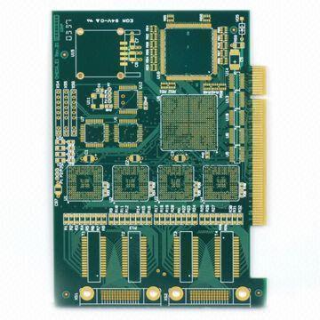
A printed circuit board (PCB) is a thin board "printed" with electrical wires and made from fiber glass or similar material. PCBs are commonly used in computer devices such as motherboards, network interface cards, and RAM chips. They are relatively cheap and quite fast. When the PCB is fabricated with several layers placed over one another, it is known as a multilayer PCB. The multiple layers establish a reliable set of predetermined interconnections for the electronic circuits.
There are several techniques that can be used to accomplish this task. Some of these techniques are handicapped by their reliance on a large number of chemical processes to condition the substrate. A large number of chemical processes are needed to activate the through-holes and electrolytic copper plate between the adjacent layers. The general procedure is as follows:
- Obtaining the material and equipment that you will need, such as drills and electrolytic copper-plating cell.
- Formatting the copper substrates so that the orientation of each can be uniquely determined. This is sometimes known as patterning and can be done using a variety of methods.
- Drilling the layers with specific drilling equipment to create holes or vias. These vias are plated with copper to form plated-through holes.
- Properly cleaning the copper substrates on your board.
- Electroplating the PCB substrate using acid copper electroplating.
- Laminating the multilayer board.
Under high pressure and heat, the layers fuse together. The conductors will be separated, and signals and power between layers will be connected. This technique ensures that all the layers are drilled and plated first, and then laminated. This can help reduce the number of chemical processes needed to accomplish this difficult task. Multilayer PCBs can have as many as 14 layers. However, this may be quite expensive, and it is more common for PCBs to have either 6 or 8 layers.
A multilayer PCB contains two reference planes and a signal via. The signal via allows a signal to flow through all the planes. A stitching via is connected to one of the planes next to the signal via and serves to reduce the area through which the signal passes through. This is very important as it may assist in reducing noise and cross talk.
Product functionality of the multilayer PCB depends on the interconnection between the layers. Thus it is very critical to be concerned about microvias and overall HDI.
Multilayer boards can either be rigid or flexible. Rigid multilayer PCB technology can prove to be very expensive because of the expertise required and the expensive drilling equipment. Flexible multilayer PCBs make use of flexible circuits and reduce the size of the end product. However, flexible multilayer PCBs must have fewer layers because an increase in the number of layers means a loss in flexibility of those layers.
Advantages of multilayer PCBs include high reliability and uniform wiring. However, the initial costs are higher than that of one-layered PCBs. Also, repairing a multilayer PCB is quite difficult.
Shane
Here is a nice video on prototyping multilayer PCBs
http://www.youtube.com/watch?v=idLpv_DjPPM